Ellipse: Do you know the orbit of planets, moon, comets, and other heavenly bodies are elliptical? Mathematics defines an ellipse as a plane curve surrounding...
Last Modified 14-04-2025

Harvest Smarter Results!
Celebrate Baisakhi with smarter learning and steady progress.
Unlock discounts on all plans and grow your way to success!

Ellipse: Definition, Properties, Applications, Equation, Formulas
April 14, 2025
Altitude of a Triangle: Definition & Applications
April 14, 2025
Manufacturing of Sulphuric Acid by Contact Process
April 13, 2025
Refining or Purification of Impure Metals
April 13, 2025
Pollination and Outbreeding Devices: Definition, Types, Pollen Pistil Interaction
April 13, 2025
Electrochemical Principles of Metallurgy: Processes, Types & Examples
April 13, 2025
Acid Rain: Causes, Effects
April 10, 2025
Congruence of Triangles: Definition, Properties, Rules for Congruence
April 8, 2025
Complementary and Supplementary Angles: Definition, Examples
April 8, 2025
Nitro Compounds: Types, Synthesis, Properties and Uses
April 8, 2025
A semiconductor diode is a \(p – n\) junction soldered with metallic contacts at the ends where an external voltage can be applied. A diode is an extremely versatile and specialized electrical component consisting of two electrodes called the anode and the cathode. Semiconductor materials like Silicon, Germanium, and Selenium are often employed for manufacturing semiconductor diodes. Some of them consist of metal electrodes in a chamber evacuated or filled with pure elemental gas at low pressure. Diodes serve various purposes, these can be employed as rectifiers, signal limiters, voltage regulators, switches, signal modulators, signal mixers, signal demodulators, and oscillators.
A semiconductor diode has a \(p-\)type semiconductor layer and the second layer of an \(n-\)type semiconductor.
A more significant number of holes are generated on doping the semiconductor materials like silicon or germanium with trivalent impurities. Hence, a layer of \(p-\)type semiconductor is created. On the other hand, if we dope semiconductor materials with pentavalent impurities, a more significant number of electrons are generated. Hence, a layer of \(n-\)type semiconductor is created. A diode is formed by joining both \(n-\)type and \(p-\)type semiconductors together. This device is created by combining \(p-\)type and \(n-\)type semiconductor material; hence it is also known as \(p – n\) Junction diode.
learn how photodiode converts light into electrical current

A two-terminal device that allows electric current flow in a single direction is known as a \(p – n\) junction diode. When the diode is forward biased, it enables the flow of electric current through it. When a reverse bias is applied across the diode, it blocks the flow of electric current through it. A \(p – n\) junction semiconductor diode is often referred to as a junction diode.

Although we can design a \(p – n\) junction diode from various semiconductor materials such as silicon, germanium, and gallium arsenide, however, for various electrical and industrial purposes, silicon is preferred over germanium. This is because the performance of \(p – n\) junction diodes made from silicon semiconductors at a higher temperature is better than the performance of \(p – n\) junction diodes made from germanium semiconductors.
A diode is a semiconductor device that essentially acts as a one-way switch for current. It allows current flow easily in one direction but severely restricts current from flowing in the opposite direction.
The polarity of a diode can be determined by its anode, i.e., the positive lead, and by its cathode, i.e., the negative lead. Diodes, in general, only allow the flow of current when the positive voltage is applied to the anode and the diode symbol’s arrow points in the direction of flow of electric current, i.e., opposite to the direction of flow of electrons.
The basic symbol of the \(p – n\) junction diode is shown in the below figure:

In the above figure, the conventional direction of electric current when the diode is forward biased, i.e., current is going from the positive terminal to the negative terminal, is indicated by the arrowhead of a diode. The holes that move from the positive terminal (anode) to the negative terminal (cathode) constitute the current’s conventional direction.
The electrons moving from the negative terminal (cathode) to the positive terminal (anode) carry the electric current. However, due to the convention, we have to assume that the current direction is from the positive terminal to the negative terminal.
The diode offers a resistance within the range of \(10\) ohms to \(1000\) ohms when it is forward-biased. When reverse-biased, an ideal diode does not allow the current to flow through it, i.e., it offers higher resistance, so when a digital multimeter is connected across it, its display will read \(OL\) (which indicates very high resistance).
A \(p-n\) junction is formed when one side of a single crystal of pure semiconductor (\(\rm{Ge}\) or \(\rm{Si}\)) is doped with acceptor impurity atoms, and the other side is doped with donor impurity atoms.

Consider the figure shown above, the \(p\) region has a high concentration of holes, and the \(n\) region contains a higher concentration of electrons. When the junction is formed, there is a movement of majority carriers across the junctions. By diffusion, the electrons from the \(n-\)side and holes from the \(p-\)side start moving across the junction. The electrons crossing the junction from \(n-\)region into the \(p-\)region recombine with holes in the \(p-\)region very close to the junction.
Similarly, holes crossing the junction from the \(p-\)region into the \(n-\)region recombine with electrons in the \(n-\)region very close to the junction. A region is generated which is depleted of any mobile charges. Thus, in this region, there won’t be any movable charge close to the junction. This region is called the depletion region. In this region, on the left side of the junction, the acceptor atoms become negative ions, and on the right side, the donor atoms become positive ions.
A standard \(p – n\) junction diode can offer two operating regions and three possible biasing conditions, and these are:
1. Zero Bias
2. Reverse Bias
3. Forward Bias

2. The forward biased condition of a \(p – n\) junction diode:
In the forward biased state, the positive terminal of the battery or power supply is connected to the \(p\) side of the device. The \(n\) side of the device is associated with the negative battery potential. Thereby causing the junction to be forward biased.

3. The reverse-biased condition of \(p – n\) junction diode:
When a power supply is connected across the diode, the \(p\) side is connected to the supply’s negative terminal. The n side is associated with the positive terminal. Then the device is said to be reverse biased.


Consider the curve shown below. The green region represents the forward-biased region of the diode, and the red curve represents the reverse-biased region of the diode.
If the diode is made from germanium, the external potential required to overcome barrier potential would be \(0.3\,\rm{V}\). As the external potential applied across the diode goes beyond \(0.3\,\rm{V}\), a rapid rise in the current is seen in the forward-biased region. It is known as the knee voltage \(V_f\). Beyond this, barrier potential is no longer necessary, and the device starts conducting as is represented by the green curve \(PQ\).

The red part of the curve represents the reverse biased condition of the device. In a reverse-biased case, the width of the depletion region is considerable. Hence, a greater barrier potential exists in the reverse-biased state. Thus, the part of the red line \(OA\) in the given curve represents the reverse saturation current that flows only due to the movement of minority charge carriers through the device, and \(AB\) represents the breakdown condition of the diode. This reverse current for a germanium diode is less than one microampere.
When a small amount of reverse voltage is applied across the diode, we can see from the curve that only a small reverse current flows through it. When the value of reverse voltage is increased beyond \(V_r\) excess amount of current flows through the diode, and this condition is known as the breakdown condition. When this condition is achieved, there will be an immediate increase in the reverse current.
A diode is a two-terminal semiconductor device that conducts electrical current in only one direction when the potential difference between its terminals exceeds a specific limit. Diodes are the most significant invention of the \(21^\rm{st}\) century & their applications are unlimited, which depends on the types of diodes. Diodes can be used as:
RECTIFIER
When a diode is forward biased, and an alternating voltage is applied, the current flows through the diode in one cycle. Due to this feature, a diode is used to rectify alternating voltages. For this purpose, it is employed in various circuits and is called a rectifier. Thus, A \(p – n\) junction diode can be used to construct different types of rectifier circuits such as half-wave, full-wave, centre-tapped, and full-bridge rectifiers.
CLIPPER
Diodes are used as clippers. A clipper circuit’s essential function is to put off the voltage beyond the preset value while ensuring that the remaining part of the input waveform remains undisturbed. These are useful in designing FM transmitters.
CLAMPER
Diodes can be used as clamper. The primary function of a clamper circuit is to shift or alter an input signal’s positive or negative peak to the desired level. Since it is used to shift the levels of the input signals, it is often referred to as a Level Shifter or \(DC\) restorer. Depending on the diode configuration, these clamping circuits can be positive or negative.
LOGIC GATE
Diodes can also perform digital logic operations. The forward and reverse-biased conditions of the diode are analogous to the low and high impedance states of a logic switch, respectively. Thus, the diode can perform logic operations such as \(AND\), \(OR\), etc. Although diode logic is an older method and encounters some limitations, these are used in various logic-based circuits. Most of the modern logic gates are \(MOSFET\) based, which is designed using multiple diodes.
VOLTAGE MULTIPLIER
A voltage multiplier is essentially a group of two or more diode rectifier circuits put together to bring \(DC\) output the same as the product of input voltages applied. Voltage doubler, tripler and quadrupler are examples of a voltage multiplier circuit. Using diodes in combination with capacitors, we get the odd or even multiple input peak voltage at the output.
VOLTAGE REGULATOR
Diodes are used in designing voltage regulator circuits. The reverse polarity can be provided by a diode which enables the current protection. It is essential to avoid the damage that occurs due to connecting the battery in a wrong way or reversing the polarities of the \(DC\) supply. The accidental connection of supply can lead to a large amount of current through the circuit components, resulting in their failure or explosion.

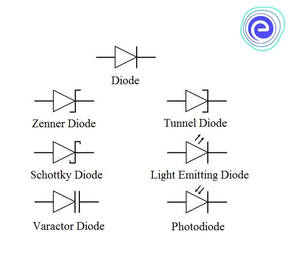
There are various types of diodes used for multiple purposes. Let us understand the types and uses of diodes.
Zener Diode: It is a type of \(p – n\) junction diode usually operated in reverse biased conditions. A Zener diode is highly used in its reverse breakdown region. It is a heavily doped \(p – n\) junction diode. It finds its application in voltage regulation, meter protection, switching, and clipping operations.
Tunnel Diode: A tunnel diode, also referred to as the Esaki diode, is a densely doped and highly conductive device. The impurity concentration of a tunnel diode is different compared to the normal \(p – n\) junction diode. It works on the principle of tunnelling and shows negative resistance characteristics.
PIN Diode: A \(3-\)layered device, called PIN diode, consists of an intrinsic region sandwiched between \(p\) and an \(n-\)type semiconductor. The presence of the intrinsic layer provides high resistivity, thus provides the key to process small input signals. These are used in microwave and radar applications.
Varactor Diode: It is commonly called a varicap diode, a combination of two words “variable” and “capacitor.” These diodes have mainly high-frequency applications, and that is why the operating mode of this diode varies with the transition capacitance, and it works in the reverse bias mode.
Photodiode: It is a diode in which current is generated when a specific region of this diode is exposed to light. Photodiodes are used in their reverse biased mode. Their uses include detection, demodulation, switching, and encoding.
LED: Light-emitting diode or LED is an electrical device in which an applied electric field results in incoherent light. LED’s are employed in various circuits in our daily life, and they are operated in a forward bias mode. LED’s are used in digital watches, phones, toys, and multimeters.
Laser Diode: LASER is the short form for Light amplification by stimulated emission of radiation. Their primary purpose is to produce coherent radiation. In telecommunications and medical applications, we often use laser diodes.
Schottky Diode: Schottky diode is not like the previous \(p – n\) junction diodes. It is formed by combining metal with an \(n-\)type semiconductor. Thus, in a Schottky diode, the depletion region is not present. These are generally used in computers and laptops.
| Vacuum Tube | Semiconductor Diode |
| • The vacuum tube is large in size and heavy in weight. • Fragile in mechanical construction. • The operation is complicated. • It has a short lifespan. • A high operating voltage is necessary. • It is primarily used in extremely high output power and high-frequency operation. | • It is small in size and light in weight. • Durable mechanical construction; no filament or heating power required • The operation is simple. • It has a very long life span. • A very low operating voltage is necessary. • It is typically used in low to medium power and frequency applications. |
A two-terminal device that allows electric current flow in a single direction is known as a \(p – n\) junction diode. When the diode is forward biased, it enables the flow of electric current through it. When a reverse bias is applied across the diode, it blocks the flow of electric current through it. A \(p – n\) junction semiconductor diode is often referred to as a junction diode. A \(p – n\) junction is formed when one side of a single crystal of pure semiconductor \((\rm{Ge}\) or \(\rm{Si})\) is doped with acceptor impurity atoms, and the other side is doped with donor impurity atoms. Diodes, in general, only allow the flow of current when the positive voltage is applied to the anode and the diode symbol’s arrow points in the direction of flow of electric current, i.e., opposite to the direction of flow of electron.
A standard \(p – n\) junction diode can offer two operating regions and three possible biasing conditions.

Q.1. List the uses of a diode.
Ans: A \(p – n\) junction diode can be used:
1. As a rectifier
2. As a switch
3. As a demodulator
4. As a Sensor
Q.2. What are types of diodes?
Ans: There are several types of diodes that we use in our day-to-day lives, some of them are:
1. Light Emitting Diode
2. Laser diode
3. Avalanche diode
4. Zener diode
5. Schottky diode
6. Photodiode
7. \(p – n\) junction diode
Q.3. What is diode explain?
Ans: An electronic component made of semiconductor material that allows current flow in only one direction is termed a Diode. A two-terminal device is typically formed by fusing \(p\) and \(n-\)type semiconductor materials, each having majority and minority carriers.
Q.4. How do diodes work?
Ans: Electrons are the majority charge carriers in the \(n-\)type region, and holes are the majority charge carrier in the \(p-\)type region. Due to the difference in concentration difference of majority charge carriers across the junctions, they diffuse across the junction and recombine with the opposite charge. It leads to the formation of positive or negative ions. These ions are collected at the junction, creating a depletion region.
1. When we connect the battery across the diode such that the connection of anode is made with the negative terminal and the cathode connection is made with the negative terminal, the diode is reverse biased.
2. Similarly, when we connect a battery across the diode such that the connection of anode is made with a positive terminal and the cathode’s connection with the battery’s negative terminal, the diode is forward-biased.
Q.5. Why is it called diode?
Ans: The word ‘diode’ is composed of two words: “\(Di\)” \(=\) \(\rm{Two}\), and “\(Ode\)” \(=\) \(\rm{Electrodes}\), i.e., a device or component comprising two electrodes which are the anode – the positive electrode \((p)\) and cathode – the negative electrode \((n)\).
Q.6. Are diodes \(AC\) or \(DC\)?
Ans: Diodes are unidirectional devices, and they conduct only when they are forward biased. Diodes work on \(DC\) as they allow the current to pass through them only in one direction. When an \(AC\) signal is applied across the diode, it conducts only during half of the cycle and blocks during the other half.
We hope you find this article on Diodes helpful. In case of any queries, you can reach back to us in the comments section, and we will try to solve them.