
Embibe Experts Solutions for Chapter: Semiconductor Electronics: Materials, Devices and Simple Circuits, Exercise 1: Gujarat Board-2018
Embibe Experts Physics Solutions for Exercise - Embibe Experts Solutions for Chapter: Semiconductor Electronics: Materials, Devices and Simple Circuits, Exercise 1: Gujarat Board-2018
Attempt the free practice questions on Chapter 14: Semiconductor Electronics: Materials, Devices and Simple Circuits, Exercise 1: Gujarat Board-2018 with hints and solutions to strengthen your understanding. EMBIBE CHAPTER WISE PREVIOUS YEAR PAPERS FOR PHYSICS solutions are prepared by Experienced Embibe Experts.
Questions from Embibe Experts Solutions for Chapter: Semiconductor Electronics: Materials, Devices and Simple Circuits, Exercise 1: Gujarat Board-2018 with Hints & Solutions
When will the conductivity of a Ge semiconductor decrease?
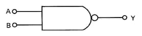
Given figure is a symbol of which logic gate?
For an N-P-N transistor in a common base circuit about of the electron entering the base from the emitter recombines with the hole. This results in the collector current being . Calculate the emitter current.
is the maximum voltage between the ends of the secondary terminal of a transformer used in a half-wave rectifier. When the P-N junction diode is reverse biased, What will be the potential difference between the two ends of the diode?
The emitter junction of the CE transistor amplifier is ______ biased while the collector junction is _____ biased.
If for a CE transistor amplifier circuit. The input resistance is equal to and the load resistance is equal to to , the voltage gain of the circuit is
:
Draw the circuit diagram of the full-wave rectifier and explain the working of the circuit.
In a N-P-N transistor about electrons enter the emitter in when it is connected to a battery. About electrons recombine with the holes in the base. Calculate the value of


