
Embibe Experts Solutions for Chapter: Electronic Devices Semiconductors, Exercise 3: Level 3
Embibe Experts Physics Solutions for Exercise - Embibe Experts Solutions for Chapter: Electronic Devices Semiconductors, Exercise 3: Level 3
Attempt the practice questions on Chapter 22: Electronic Devices Semiconductors, Exercise 3: Level 3 with hints and solutions to strengthen your understanding. Physics Crash Course JEE Main solutions are prepared by Experienced Embibe Experts.
Questions from Embibe Experts Solutions for Chapter: Electronic Devices Semiconductors, Exercise 3: Level 3 with Hints & Solutions
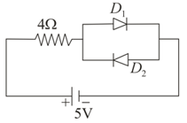
In the network shown,
The width of depletion region in a $p$-$n$ junction diode is and an intense electric field of . Then, potential barrier is,
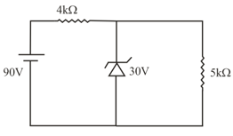
The zener diode has a The current passing through the diode for the following ciruit is __________ .
In a amplifier, the input ac signal to be amplified is applied across
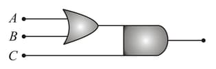
To get an output from the circuit shown below the input must be
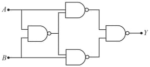
The truth table for the system of four gate as shown in the figure is
A signal of is transmitted in a cable. The attenuation of cable is and cable length is the power received at receiver is . The value of is Gain in
On a particular day, the maximum frequency reflected from the ionosphere is . On next day it was found to increase to . If ratio of maximum electron densities of first day to maximum electron densities of next day the ionosphere is . find value of .


