
Draw the diagram for transistor being used as a switch.
Important Questions on Semiconductor Devices
An n-p-n transistor has three leads A, B and C. Connecting B and C by moist fingers, A to the positive lead of an ammeter, and C to the negative lead of the ammeter, one finds large deflection. Then, A, B and C refer respectively to :
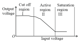
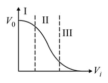
The transfer characteristics for a transistor in mode is as shown in figure. To use transistor as a switch, it should be used in
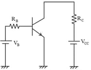
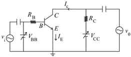
In the figure, given that supply can vary from to and The minimum base current and the input voltage at which the transistor will go to saturation, will be, respectively:
Given below are two statements : One is labelled as Assertion A and the other is labelled as Reason R.
Assertion(A) : transistor permits more current than a transistor.
Reason(R) : Electrons have greater mobility as a charge carrier.


