
MEDIUM
Earn 100
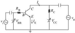
The correct circuit for a pnp transistor amplifier in common emitter configuration :-
50% studentsanswered this correctly
Important Questions on Semiconductor Devices
MEDIUM
MEDIUM
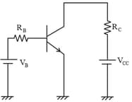
In the figure, given that supply can vary from to and The minimum base current and the input voltage at which the transistor will go to saturation, will be, respectively:
EASY
MEDIUM
EASY
EASY
EASY
EASY
MEDIUM
EASY
EASY
MEDIUM
MEDIUM
HARD
MEDIUM
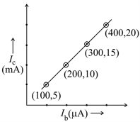
The transfer characteristic curve of a transistor, having input and output resistance and respectively, is shown in the figure. The voltage and power gain, are respectively:
EASY
MEDIUM
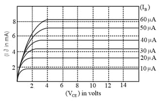
The output characteristics of a transistor is shown in the figure. When is and , then value of is
MEDIUM
An n-p-n transistor has three leads A, B and C. Connecting B and C by moist fingers, A to the positive lead of an ammeter, and C to the negative lead of the ammeter, one finds large deflection. Then, A, B and C refer respectively to :
EASY
EASY


