
EASY
Earn 100
What are input characteristics of common emitter transistor?
Important Questions on Semiconductor Devices
MEDIUM
An n-p-n transistor has three leads A, B and C. Connecting B and C by moist fingers, A to the positive lead of an ammeter, and C to the negative lead of the ammeter, one finds large deflection. Then, A, B and C refer respectively to :
MEDIUM
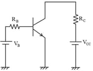
Draw the circuit arrangement for studying the output characteristics of n-p-n transistor in CE configuration. Explain how the output characteristics is obtained.
EASY
In a common-emitter transistor amplifier, the audio signal voltage across the collector is The resistance of collector is . If current gain is and the base resistance is , the voltage and power gain of the amplifier is
HARD
A realistic graph depicting the variation of the reciprocal of input resistance in an input characteristics measurement in a common emitter transistor configuration is :
EASY
The input signal is given to a CE amplifier having a voltage gain of is . The corresponding output signal will be:
EASY
An unknown transistor needs to be identified as a or type. A multimeter, with +ve and -ve terminals, is used to measure resistance between different terminals of transistor. If terminal 2 is the base of the transistor then which of the following is correct for a transistor?
MEDIUM
The current gain of a common emitter amplifier is . If the emitter current is , collector current is :
MEDIUM
An transistor is used in common emitter configuration as an amplifier with load resistance. Signal voltage of is applied across the base-emitter. This produces a change in the collector current and change in the base current of the amplifier. The input resistance and voltage gain are:
MEDIUM
For common emitter transistor amplifier, the audio signal voltage across the collector resistance of is If the current amplification factor of the transistor is and the base resistance is then the input signal voltage is
EASY
In a common emitter amplifier circuit using an transistor, the phase difference between the input and the output voltages will be:
EASY
The ratio (R) of output resistance and the input resistance in measurements of input and output characteristics of a transistor is typically in the range :
MEDIUM
A NPN transistor is connected in common emitter configuration in a given amplifier. A load resistance of is connected in the collector circuit and the voltage drop across it is . If the current amplification factor is and the input resistance of the circuit is , the voltage gain and the power gain of the amplifier will respectively be:
MEDIUM
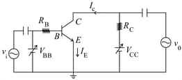
A common emitter amplifier circuit, built using an NPN transistor, is shown in the figure. Its dc current gain is , and . The minimum base current for to reach saturation is
EASY
For a common emitter configuration, if and have their usual meanings, the correct relationship between and is:
EASY
An transistor operates as a common emitter amplifier, with a power gain of . The input circuit resistance is and the output load resistance is . The common emitter current gain is:
EASY
In the study of transistor as an amplifier, the ratio of collector current to emitter current is then the ratio of collector current to base current will be
MEDIUM
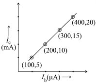
The transfer characteristic curve of a transistor, having input and output resistance and respectively, is shown in the figure. The voltage and power gain, are respectively:
EASY
For a transistor, and are the current ratios, then the value of is
MEDIUM
In the figure, given that supply can vary from to and The minimum base current and the input voltage at which the transistor will go to saturation, will be, respectively:
HARD
Draw a neat circuit diagram to study the input and output characteristics of a common emitter transistor.


