Junction Transistor
Junction Transistor: Overview
This topic covers concepts, such as, Junction Transistor, Symbol of a Transistor, Current Transfer Characteristics in Common Emitter Configuration Transistor & Transistor Biasing etc.
Important Questions on Junction Transistor
Choose the correct expression for the current gain in n – p – n transistor in CE configuration:
Choose the correct expression for the current gain in n – p – n transistor in CE configuration:
Output is taken between the emitter and the base of a transistor in a common-collector configuration of an amplifier.
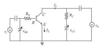
Show the circuit diagram for the biasing of a P-N-P transistor in common collector configuration.
Draw the circuit diagram for the common collector configuration of N-P-N transistor as an amplifier.
The relationship between current gain in Common Base [CB] mode and current gain in Common Emitter [CE] mode is
A transistor having and is given in the circuit. Find the value of the collector current.
________ segment supplies the majority charge carriers for the current flow through a transistor
The base region in a p-n-p transistor is obtained by doping an intrinsic semiconductor with
The moderate sized and heavily doped region of a transistor is
What will be the current gain in the common emitter amplifier if
In an NPN transistor circuit, the collector current is If of the emitted electrons reach the collector, the emitter current and base current are given by
The input signal is given to a CE amplifier having a voltage gain of is . The corresponding output signal will be:
For a common emitter configuration, if and have their usual meanings, the correct relationship between and is:
The ratio (R) of output resistance and the input resistance in measurements of input and output characteristics of a transistor is typically in the range :
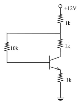
In the figure, given that supply can vary from to and The minimum base current and the input voltage at which the transistor will go to saturation will be, respectively:
A transistor connected at common emitter mode contains load resistance of and an input resistance of If the input peak voltage is and the current gain is find the voltage gain.
In the circuit shown in the figure, the input voltage is , and . Fint the values of , and :
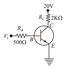
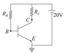
For given biasing circuit, if the voltage across collector-emitter is and current gain is and base current is then determine the value collector resistance
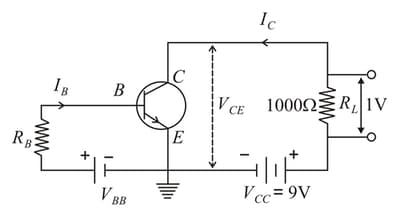
An N-P-N transistor is connected in a common emitter configuration in which collector supply is and the voltage drop across the load resistance of connected in the collector circuit is . If the current amplification factor is . If the internal resistance of the transistor is , then which of the following options is incorrect.